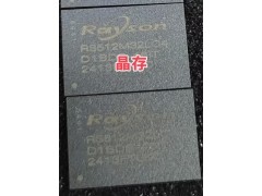
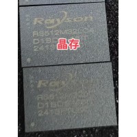
Features
This data sheet is for LPDDR4X and LPDDR4
unified product based on LPDDR4X information.
As for LPDDR4 setting, refer to General LPDDR4
Specification at the end of this datasheet.
• Ultra-low-voltage core and I/O power supplies
- V
DD1
= 1.70-1.95V; 1.80V nominal
- V
DD2
= 1.06-1.17V; 1.10V nominal
- V
DDQ
= 0.57-0.65V; 0.60V nominal
Or V
DDQ
= 1.06-1.17V; 1.10V nominal
• Frequency range
- 2133-10 MHz (data rate range per pin:4266-20
Mb/s)
• 16 n prefetch DDR architecture
• 8 internal banks per channel for concurrent
operation
• Single-data-rate CMD / ADR entry
• Bidirectional / differential data strobe per byte
lane
• Programmable READ and WRITE latencies (RL
/ WL)
• Programmable and on-the-fly burst lengths (BL =
16, 32)
• Directed per-bank refresh for concurrent bank
operation and ease of command scheduling
• Up to 8.53 GB / s per die x16 channel
• On-chip temperature sensor to control self refresh
rate
• Partial-array self refresh (PASR)
• Selectable output drive strength (DS)
• Clock-stop capability
• RoHS-compliant, “green” packaging
• Programmable V
SS
(ODT) termination
• Single-ended CK and DQS support


 客服热线:
客服热线:


&tel=15914053950&work=0755-83685114&email=&org=深圳市鑫融宸电子有限公司&adr=深圳市龙华区民治街道上芬社区人民路恒江大厦1302&url=https://www.oemao.com/com/xrc01/)