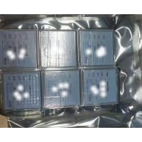
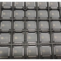
K4A8G165WB-BCRC
Information
• JEDEC standard 1.2V (1.14V~1.26V)
• VDDQ = 1.2V (1.14V~1.26V)
• VPP = 2.5V (2.375V~2.75V)
• 800 MHz fCK for 1600Mb/sec/pin, 933 MHz fCK for 1866Mb/sec/pin,
1067MHz fCK for 2133Mb/sec/pin, 1200MHz fCK for 2400Mb/sec/pin,
1333MHz fCK for 2666Mb/sec/pin
• 8 Banks (2 Bank Groups)
• Programmable CAS Latency(posted CAS):
10,11,12,13,14,15,16,17,18,19,20
• Programmable CAS Write Latency (CWL) = 9,11 (DDR4-1600) , 10,12
(DDR4-1866) ,11,14 (DDR4-2133) ,12,16 (DDR4-2400) and 14,18 (DDR4-
2666)
• 8-bit pre-fetch
• Burst Length: 8, 4 with tCCD = 4 which does not allow seamless read or
write [either On the fly using A12 or MRS]
• Bi-directional Differential Data-Strobe
• Internal(self) calibration : Internal self calibration through ZQ pin
(RZQ : 240 ohm ± 1%)
• On Die Termination using ODT pin
• Average Refresh Period 7.8us at lower than TCASE 85C, 3.9us at 85C <
TCASE < 95 C
• Support Industrial Temp ( -4095C )
- tREFI 7.8us at -40 °C ≤ TCASE ≤ 85°C
- tREFI 3.9us at 85 °C < TCASE ≤ 95°C
• Asynchronous Reset
• Package : 96 balls FBGA - x16
• All of Lead-Free products are compliant for RoHS
• All of products are Halogen-free
• CRC(Cyclic Redundancy Check) for Read/Write data security
• Command address parity check
• DBI(Data Bus Inversion)
• Gear down mode
• POD (Pseudo Open Drain) interface for data input/output
• Internal VREF for data inputs
• External VPP for DRAM Activating Power
• PPR and sPPR is supported
K4A4G165WF-BIWE
Information
4Gb/256M*16/3200MBbps/12V/ -40~95度/96 FBGA/


 客服热线:
客服热线:


&tel=15914053950&work=0755-83685114&email=&org=深圳市鑫融宸电子有限公司&adr=深圳市龙华区民治街道上芬社区人民路恒江大厦1302&url=https://www.oemao.com/com/xrc01/)